1. Introduction
Terahertz (THz) radiation, in between the millimeter-wave (100 GHz) and far infra-red (10 THz) regions of the electromagnetic spectrum, displays many unique properties, such as a strong sensitivity to polar liquids [
1], high transmission through a range of non-conducting materials [
2,
3], and spectroscopic responses to many materials [
4]. These features can be applied to medical imaging and diagnosis (for example, detecting skin cancers beneath the skin due to increased water content in tumour cells [
5]), remote detection of explosive substances and drugs through spectroscopic response of crystalline compounds [
3,
6], and non-destructive imaging of items concealed in optically opaque packaging [
2,
3,
7]. Recent research and achievements in THz technology are summarized in a number of review papers [
4,
7,
8].
Since THz imaging was first demonstrated in the mid-90s [
9], various technologies have been explored for this application over the past two decades. Different system architectures were built depending on what types of sources, detectors and other components were accessible. For example, typical optical-approached systems are based on various laser sources (femtosecond optical pulses, semiconductor lasers, and quantum cascade lasers) to generate and tune THz signals and photoconductive or photosensitive materials to detect/receive the signals. Time domain spectroscopic imaging and monochromatic imaging (continuous-wave (CW) imaging) [
4,
6,
9,
10] have been recognized as promising methods, especially for non-destructive inspection and materials analysis. Solid-state electronic component-based imaging systems have also been developed based on various microwave electronic components. Virginia Diodes Inc. (Charlottesville, VA, USA;
http://vadiodes.com) has now offered a range of relatively mature and compact THz products such as amplifier multiplier chain THz sources and diode detectors enabling potentially compact high-performance all-electronics systems. These electronic THz imaging systems, typically in sub-THz frequency ranges, are promising for variety practical applications (for example [
11]). Optic scheme is commonly used to direct and couple the THz signal to the specimen and the detector [
11,
12,
13]. Since the solid-state electronic devices are fabricated by planar micro-lithographic processing techniques, they can be easily scaled up to large array devices for multi-pixel imaging. It is not however the purpose of this paper to provide an extensive overview of various imaging technologies, and reference [
7] gives a good summary and comparison of a range of imaging technologies.
Until recent advances in THz sources and detectors, there has been a lack of low cost commercial high-performance THz instruments. Most of the THz systems presented in the literature are laboratory bench-top demonstrators; complex, bulky, difficult to operate and impossible to move. For wide adoption of THz technology to occur, the systems will have to become more compact, affordable and user friendly, which requires new approaches to many details of the components and system architectures. Some recent progress in emerging commercial THz instruments is worth mentioning. For example, Lake Shore Cryotronics, Inc. (Westerville, OH, USA;
www.lakeshore.com) and QMC Instruments Ltd. (Billingshurst, UK;
www.terahertz.co.uk/qmc) have offered cryogenically cooled THz spectrometers for materials characterisation, but the instruments are still bulky and expensive. Advantest Co. (Tokyo, Japan;
www.advantest.com) offers a series of spectroscopic analysis systems. TeraSense Group (San Jose, CA, USA;
www.terasense.com) has presented a number of THz spectroscopy systems and very recently the sub-THz imaging camera. Despite this progress, available commercial high-performance and low cost THz systems, especially imaging systems (available commercial systems are mostly spectroscopy systems), are still scarce and high cost, preventing widespread use of THz technology. Continuing research and development of THz instruments is anticipated to further drive the system costs down and promote application of the THz technology.
CSIRO has in recent years developed electronic component-based THz imaging systems [
12,
13], antenna-coupled integrated THz detectors [
14] and sensitive superconducting detectors [
15,
16,
17]. The previous imaging system, though producing excellent images, employed a large size backward-wave oscillator (BWO) THz source and a series of more expensive and harder to align optical mirrors to form a quasi-optical active imaging system. The system was too bulky and complicated to operate. The motivation of this work was to develop a more compact, lower cost, user-friendly and industry-adaptable imaging system. We have employed more compact state-of-the art solid-state THz components, explored various beam guiding architectures and have built a practical and simpler imaging system that could be readily applied to imaging in either transmission or reflection mode according to the desired application.
2. Experimental Setup—Hardware and System Configurations
Moving to a more compact system, we have first made various changes to the hardware components. The previous BWO THz source was replaced with a much more compact state-of-the art solid-state 625 GHz Amplifier/Multiplier chain (AMC) from Virginia Diodes Inc. It generates CW radiation between 590 and 650 GHz with a maximum output of around 1 mW. While the output power is less than that produced by the BWO (10 mW maximum), certain limitations of the BWO such as a finite lifespan of approximately 1000 h are overcome. The BWO has a nonstandard size output waveguide close to WR10 leading to the guide being overmoded at the test frequencies, which results in a non-ideal amplitude distribution across the collimated beam (see Figure 9a in [
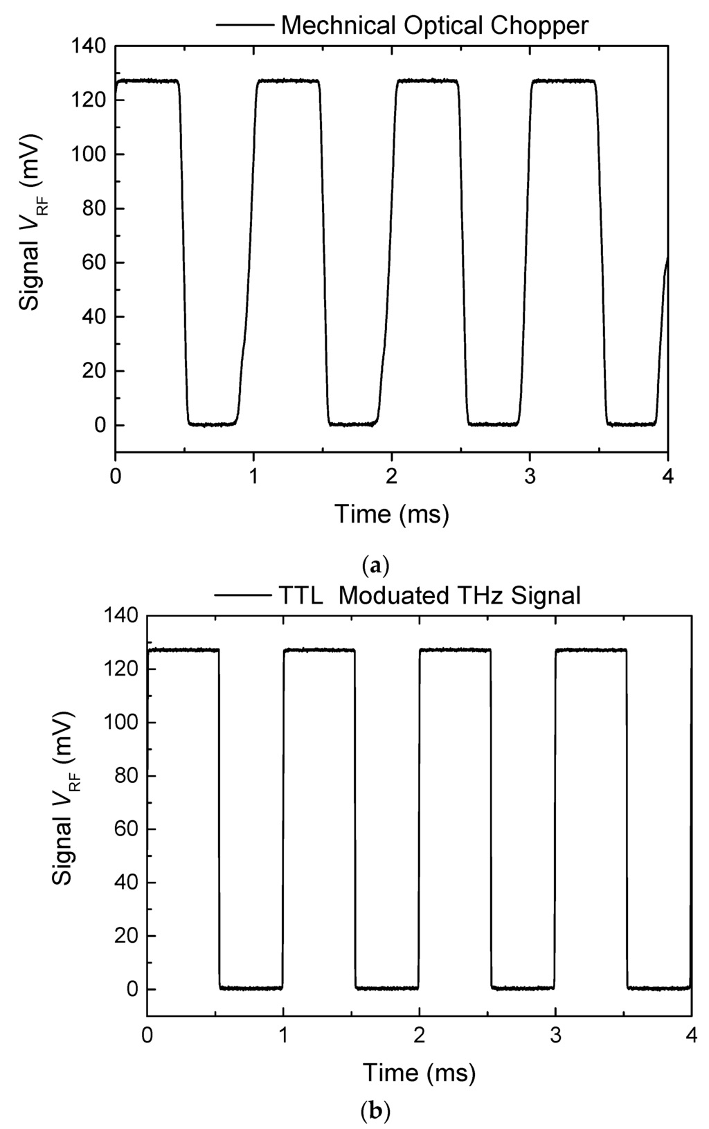
18]). The new solid-state AMC source does not have this overmoding issue as it has appropriately sized WR1.5 waveguide and diagonal waveguide horn with approximately 25 dB of gain. The source is also frequency sweepable and comes with a TTL modulation port. A compact economy synthesizer, instead of a standalone bench top RF signal generator, was used to supply the input signal for the AMC THz source and it offers digital tuning via LabVIEW by the system control computer. The AMC and compact synthesizer represent a great advantage over both the size, weight and complexity of the previous BWO system.
Virginia Diodes WR-1.5ZBD Zero-bias Schottky diode detectors were used to receive the transmitted or reflected signals from the sample. The detectors were mounted on a precision XY translation mounts allowing for fine adjustment of detector to optical lens alignment. The XY translator provides ±2 mm of travel perpendicular to the optical axis.
The THz imager is a quasi-optical active imaging system comprising collimating and focusing mirrors. Mirrors were used to focus the THz beam onto the sample and then onto the detector. Precision lens alignment and maintenance of these aligned lenses are important for maximizing the beam signal or signal-to-noise ratio thus obtaining the best quality images. Off-axis parabolic mirrors were used in our earlier imaging system [
12,
13,
14,
15,
16]. They proved difficult and time consuming to align and realign after any movement or relocation or change of system configuration for different measurements. The off-axis parabolic mirrors were replaced with plano-convex Teflon PTFE lenses in our current new system which employed a linear arrangement of the lenses. The PTFE lenses offer the benefits of easier alignment and to a lesser extent lower cost, at only 10% of the cost of the parabolic optical mirrors. Experiments were carried out to compare both types of lenses and the beam alignment schemes. We obtained similar detectable signal amplitude and signal-to-noise ratio (SNR) from both. Although the PTFE lenses have higher loss than that of the off-axis mirrors, a simpler and better beam alignment compensated the loss. One disadvantage of the PTFE lenses over the mirrors is that visible light does not go through and therefore cannot be used for coarse alignment. This disadvantage was partially fixed in our system as described in next section by locking in all the lenses (and the detector) in the same axis, and thus removed the need for coarse alignment (only the focal distance needs fine adjustment which can be monitored with the detector signal level).
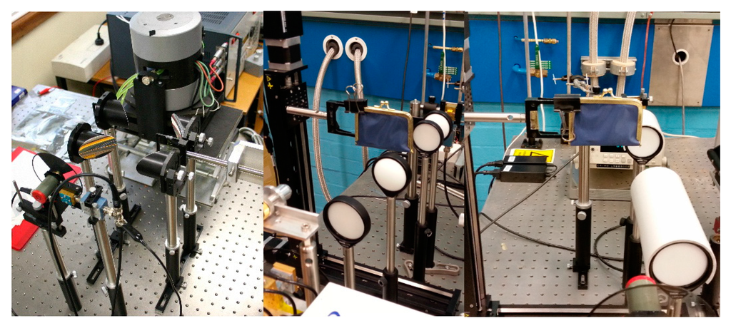
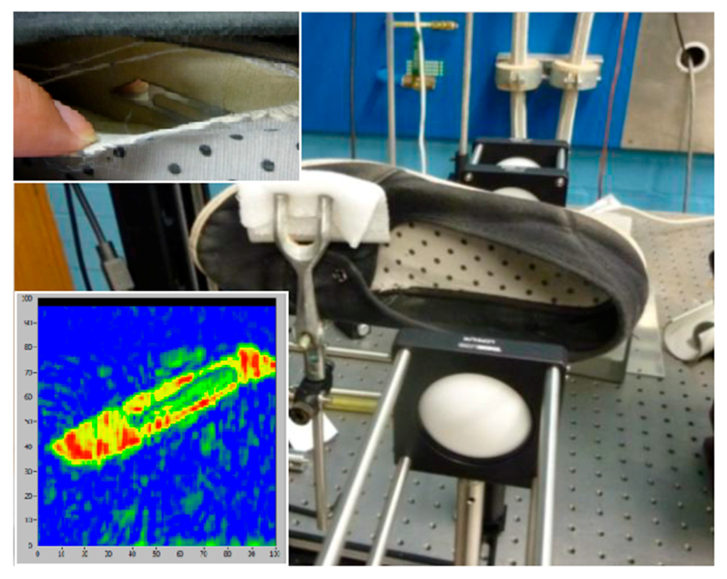
Figure 1 shows the examples of our quasi-optical transmission imaging system improvement process. The left photograph is our earlier system using the BWO source and the off-axis parabolic mirrors. The middle picture shows a linear lens alignment scheme using the plano-convex PTFE lenses for testing the beam alignment and the image quality. The picture on the right shows the further improvement by locking in all the lenses in the same axis, i.e., reducing the freedom of the movement of individual lens using a in-house fabricated PVC circular cover. Changing from the off-axis alignment to the linear system has significantly simplified the system and reduced the time required to realign the beam after the system being moved or the configuration being changed.
Figure 1. Examples of the system improvement steps with varied hardware and the beam guiding schemes.
Figure 2 shows the final imaging system mounted on a portable plate without the cover. It employs a lens cage-system to lock the linear-aligned lens and is switchable between transmission and reflection imaging mode. We also designed a removable beam splitter fitted into a lens mounting cube (see
Figure 2 inset) as part of the lens alignment system so the system can be easily switched from the transmission to a reflection mode. The beam splitter consists of a high resistivity float zone 0.5 mm thick silicon wafer. High resistive silicon is one of the only isotropic crystalline materials with a wide bandwidth of operation, maintaining up to 50%–54% transmission at millimetre and terahertz waves. The complete imaging system hardware is shown in
Figure 2 from left to right; source, beam splitter mount (cube), reflection mode detector in a mount perpendicular to the transmission path, the frequency synthesizer above the detector, collimation and focusing lenses, the XY sample scanner, and the transmission mode detector mounted in a precision XY translation mount.
Figure 2. A view of the full system mounted on a portable optical plate (450 mm × 750 mm) showing a linearly aligned source-lenses-sample-detector scheme and a removable beam splitter (inset) for changing between transmission and reflection mode.
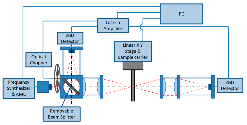
The operation schematic diagram is shown in
Figure 3 which illustrates how the current THz imaging system is configured. As discussed the system employs a caged lens-mounting set-up where the plano-convex PTFE lenses are mounted in a cage system formed by parallel rods. The cage mounting locks all lenses on a single axis thus reducing the freedom of individual lens movement and achieving the best lens alignment. The rigid lens mounting simplifies the alignment of the source beam to sample and then to detector and produce more robust imaging system. The system can now be moved and realigned in a matter of minutes if need be. The advantages of using such a rigid cage mounting scheme have also been recognised by Hoyer et al. [
19] in their portable THz scanner for structural inspection of buildings.
Figure 3. Schematic of the quasi-optical THz transmission and reflection imaging system.